← How to Create PCB Layouts in Proteus: Beginner's Tutorial! Design circuits schematics and pcb layouts in proteus, easyeda and 15 DIY Coffee Roaster Arduino Ideas: Home Brewing Hacks! Number fifteen →
If you are looking for The PCB Layout "Rules of Thumb" and Guidelines Debate Rages On you've visit to the right page. We have 25 Images about The PCB Layout "Rules of Thumb" and Guidelines Debate Rages On like Review of Server PCB Layout & Schematic – Part 4: PCI Express (PCIE), PCB layout rules for PCIE, SATA, LAN, LVDS, USB, SDVO, and also The PCB Layout "Rules of Thumb" and Guidelines Debate Rages On. Read more:
The PCB Layout "Rules Of Thumb" And Guidelines Debate Rages On
 resources.altium.com
The PCB Layout "Rules of Thumb" and Guidelines Debate Rages On
PCB Layout Rules | Sierra Circuits
 www.protoexpress.com
PCB Layout Rules | Sierra Circuits
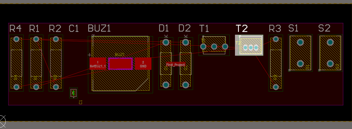
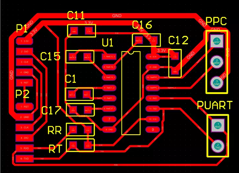
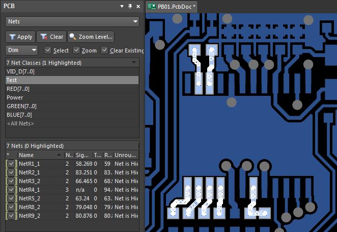
Convert Schematic To Pcb Layout
 partdiagramsibalekepg.z19.web.core.windows.net
Convert Schematic To Pcb Layout
Convert Schematic To Pcb Layout
 usermanualaduncity.z13.web.core.windows.net
Convert Schematic To Pcb Layout
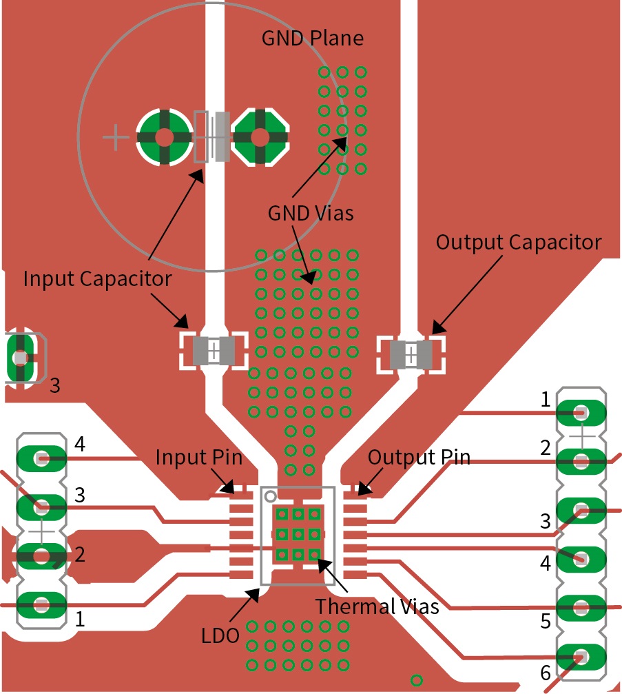
Voltage - Output Capacitor PCB Layout - Electrical Engineering Stack
 electronics.stackexchange.com
voltage - Output capacitor PCB layout - Electrical Engineering Stack ...
Review Of Server PCB Layout & Schematic – Part 4: PCI Express (PCIE)
 www.fedevel.com
Review of Server PCB Layout & Schematic – Part 4: PCI Express (PCIE)
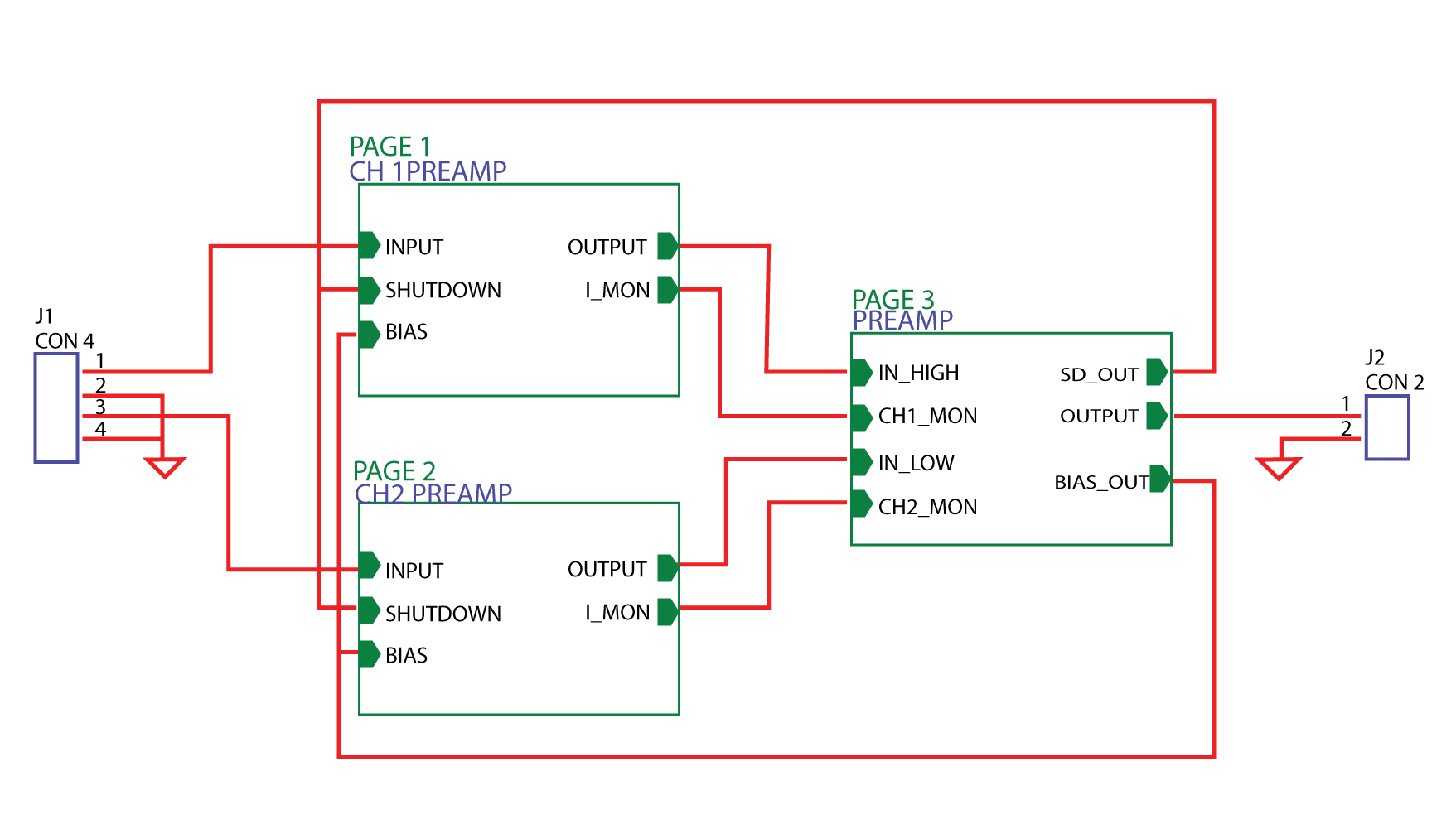
Pcb Schematic And Layout
 circuitlibgromets.z13.web.core.windows.net
Pcb Schematic And Layout
The PCB Layout "Rules Of Thumb" And Guidelines Debate Rages On
 resources.altium.com
The PCB Layout "Rules of Thumb" and Guidelines Debate Rages On
[DIAGRAM] Molex To Pcie Adapter Wiring Diagram Schematic - WIRINGSCHEMA.COM
![[DIAGRAM] Molex To Pcie Adapter Wiring Diagram Schematic - WIRINGSCHEMA.COM](https://gergely.imreh.net/blog/wp-content/uploads/2015/08/pcieduino_schematic.png) wiringschema.com
wiringschema.com
[DIAGRAM] Molex To Pcie Adapter Wiring Diagram Schematic - WIRINGSCHEMA.COM
13 Basic Rules Of PCB Layout
 www.raypcb.com
13 Basic Rules Of PCB Layout
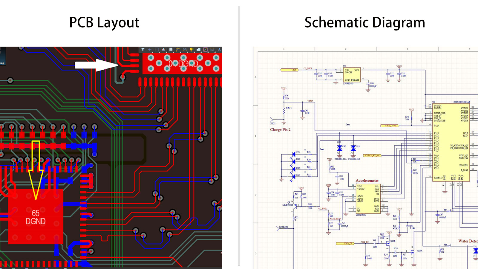
PCB Schematic Vs PCB Layout
 www.nextpcb.com
PCB Schematic vs PCB Layout
PCB Layout Rules - Exhibition - News
 www.oem-pcb.com
PCB Layout Rules - exhibition - News
How To Read A Pcb Schematic
 schematicpinier.z13.web.core.windows.net
How To Read A Pcb Schematic
PCB Layout Rules For PCIE, SATA, LAN, LVDS, USB, SDVO,
 www.fedevel.com
PCB layout rules for PCIE, SATA, LAN, LVDS, USB, SDVO,
PCB Layout Rules For PCIE, SATA, LAN, LVDS, USB, SDVO,
 www.fedevel.com
PCB layout rules for PCIE, SATA, LAN, LVDS, USB, SDVO,
PCB Design Rules - Build Electronic Circuits
 www.build-electronic-circuits.com
PCB Design Rules - Build Electronic Circuits
Ddr3 Pcb Layout Rules - PCBSky
 www.pcbsky.com
Ddr3 pcb layout rules - PCBSky
Pcb Layout Design Rules.pdf Keelegerh
 lotyvanla.weebly.com
Pcb Layout Design Rules.pdf keelegerh
Schematic To Pcb Design
 schematicpartchar.z21.web.core.windows.net
Schematic To Pcb Design
PCB Layout Rules And Guidance - PCB & PCBA Manufacturer
 ipcb.co
PCB layout rules and guidance - PCB & PCBA Manufacturer
PCB Design Layout Rules Recommendations - AiPCBA
 www.aipcba.com
PCB Design Layout Rules Recommendations - AiPCBA
PCB Layout Rules
 www.linkedin.com
PCB layout rules
PCB Layout Rules For PCIE, SATA, LAN, LVDS, USB, SDVO,
 www.fedevel.com
PCB layout rules for PCIE, SATA, LAN, LVDS, USB, SDVO,
Ten Golden Rules Of PCB Design & Its Guidelines
 absolutepcbassembly.com
Ten Golden Rules of PCB Design & its Guidelines
The PCB Layout "Rules Of Thumb" And Guidelines Debate Rages On
 resources.altium.com
The PCB Layout "Rules of Thumb" and Guidelines Debate Rages On
Pcb layout rules for pcie, sata, lan, lvds, usb, sdvo,. Ddr3 pcb layout rules. The pcb layout "rules of thumb" and guidelines debate rages on